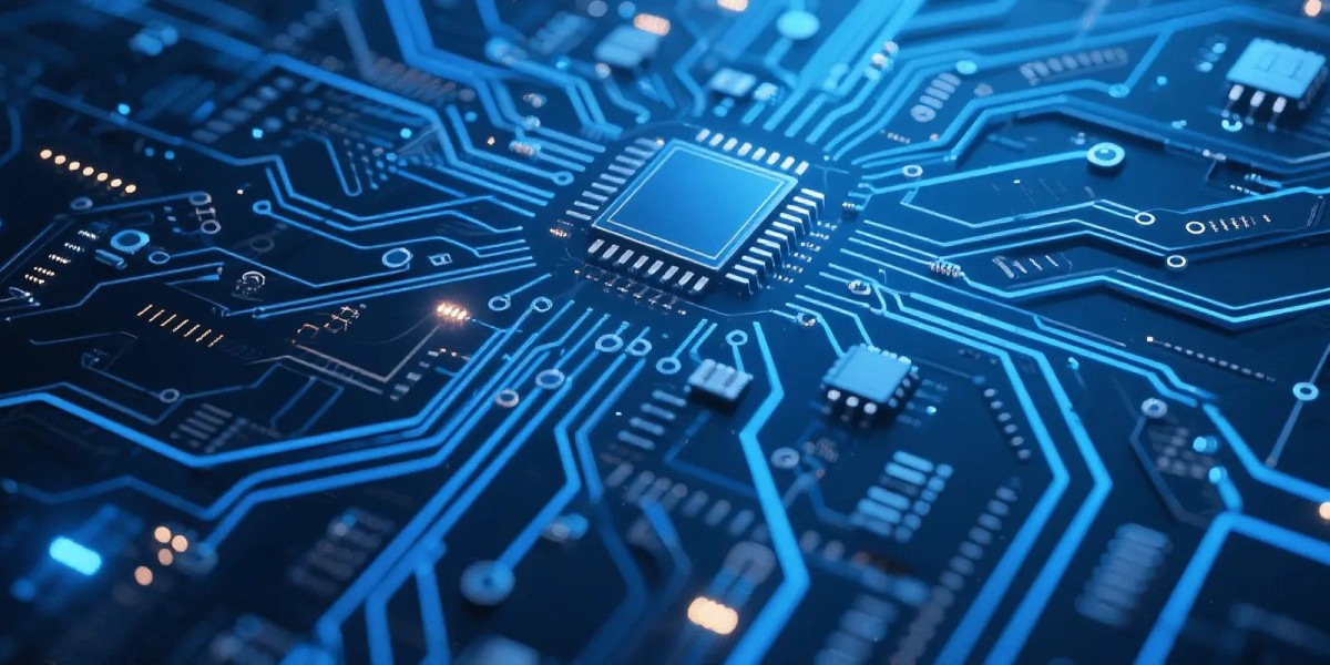
Printed circuit board production is a highly detailed process that depends on precise technical documentation. A completed PCB layout alone is not enough to begin manufacturing because fabrication and assembly facilities require multiple supporting files to understand how the board should be produced. In this process, knowing the purpose of Required PCB Files is important because these files contain the information necessary for accurate fabrication, drilling, assembly, and testing.
Modern PCB manufacturing involves several interconnected stages, including copper imaging, hole drilling, solder masking, component placement, and electrical verification. Every stage relies on properly generated design outputs from PCB software. If any file is incomplete or incorrect, production quality can suffer, leading to delays, assembly problems, or expensive redesigns.
Importance of PCB Documentation in Manufacturing
PCB documentation serves as the communication channel between the design engineer and the production facility. Each file generated during the design process provides specific instructions that guide fabrication and assembly operations.
Manufacturers depend on these files to determine:
- PCB dimensions
- Copper layer layouts
- Drill hole locations
- Solder mask areas
- Component placement details
- Material specifications
Complete and accurate documentation helps ensure the final board is manufactured according to the intended design. Poor documentation can create misunderstandings that affect production quality and reliability.
Gerber Files and Their Function
Gerber files are the standard manufacturing outputs used for PCB fabrication. These files contain graphical representations of every layer in the board design.
Separate Gerber files are typically generated for:
- Top copper layer
- Bottom copper layer
- Solder mask layers
- Silkscreen layers
- Paste mask layers
Fabrication equipment uses these files to transfer circuit patterns onto the PCB material during production.
Because Gerber files directly control manufacturing processes, engineers should inspect them carefully before submission. Gerber viewing tools help verify layer alignment, trace accuracy, and completeness of exported data.
Drill Files and Hole Specifications
Drill files define the size and position of holes that must be created during PCB fabrication. These files are commonly generated in Excellon format and are used by automated drilling machines.
Drill data generally includes:
- Via holes
- Through-hole component holes
- Mounting holes
- Mechanical openings
Accurate drill information is essential because incorrect hole dimensions can cause assembly issues or unreliable electrical connections.
Designers should also confirm that plated and non-plated holes are clearly identified to avoid manufacturing confusion.
Bill of Materials for Component Assembly
The Bill of Materials, or BOM, is a document containing the complete list of components required for PCB assembly.
A typical BOM includes:
- Component values
- Reference designators
- Package types
- Quantities
- Manufacturer part numbers
Assembly teams use this information to source components and verify placement accuracy during production.
A well-organized BOM improves inventory management and reduces the risk of incorrect component installation. Including approved alternative components can also help prevent delays caused by supply shortages.
Pick and Place Files in Automated Production
Modern PCB assembly relies on automated pick and place machines capable of positioning components with high precision. These machines require coordinate data generated from the PCB layout.
Pick and place files typically contain:
- Component coordinates
- Rotation angles
- Placement side details
- Reference labels
Accurate placement data ensures efficient assembly and reduces manufacturing errors.
Before sending files to the assembly facility, engineers should verify that all component orientations and coordinate systems match the physical PCB layout.
Assembly Drawings and Production Notes
Assembly drawings provide visual guidance for technicians during component installation and inspection.
These drawings commonly show:
- Component outlines
- Polarity markings
- Connector orientation
- Reference designators
In addition, fabrication notes communicate technical manufacturing requirements such as:
- Board thickness
- Copper weight
- Surface finish type
- Solder mask color
- Special testing procedures
Clear assembly documentation helps manufacturers follow design specifications accurately and reduces production misunderstandings.
Stackup Details for Multilayer Boards
Multilayer PCB designs require stackup documentation that defines the arrangement of conductive and insulating layers within the board.
A stackup document generally includes:
- Number of layers
- Copper thickness
- Dielectric material types
- Layer spacing
- Controlled impedance values
Manufacturers use this information during lamination and material selection processes. Proper stackup planning also affects signal integrity, thermal performance, and electromagnetic compatibility.
Providing accurate stackup data helps ensure reliable electrical behavior and manufacturing consistency.
Netlist Files and Electrical Verification
Netlist files describe all electrical connections within the PCB layout. Manufacturers use these files during electrical testing to compare the fabricated board with the original design.
Electrical verification helps identify:
- Open circuits
- Short circuits
- Missing connections
- Routing defects
Netlist testing improves product reliability by detecting manufacturing problems before assembly begins.
This process is especially important for complex and high-density PCB designs.
Design Rule Checks Before Production
Before generating manufacturing outputs, engineers should perform design rule checks to identify layout issues that could affect fabrication.
Design rule verification commonly includes:
- Trace width validation
- Copper spacing checks
- Drill clearance analysis
- Annular ring verification
- Solder mask alignment inspection
Modern PCB design software includes automated tools that simplify this process and help ensure the layout meets manufacturing requirements.
Correcting design violations early helps reduce fabrication risks and improves final product quality.
Organizing PCB Files Efficiently
Proper organization of manufacturing data is essential for smooth communication with fabrication facilities. Poorly labeled files can create confusion and increase the risk of production mistakes.
Good file management practices include:
- Using clear file names
- Separating fabrication and assembly data
- Including revision numbers
- Maintaining structured project folders
Well-organized documentation allows manufacturers to process projects more efficiently and reduces delays.
Common Issues Caused by Incorrect Documentation
Incomplete or inaccurate manufacturing files can lead to serious production problems.
Common documentation errors include:
- Missing Gerber layers
- Incorrect drill dimensions
- Wrong component orientation
- Outdated BOM information
- Incomplete fabrication instructions
Even small mistakes can increase production costs and delay project timelines. Thorough verification before file submission is essential.
Revision Control in PCB Projects
PCB designs often go through multiple updates during development, making revision management an important part of the manufacturing workflow.
Proper revision control includes:
- Version numbering
- Change tracking
- Approval documentation
- Release dates
Using outdated files during production can result in incorrect fabrication and wasted resources. Accurate revision tracking helps ensure manufacturers always use the latest approved design.
Collaboration with PCB Manufacturers
Strong communication between PCB designers and manufacturers helps improve manufacturability and reduce production risks.
Manufacturers can provide guidance regarding:
- Material selection
- Minimum trace capabilities
- Drill limitations
- Panelization methods
- Assembly restrictions
Early collaboration allows potential manufacturing problems to be identified before production begins, saving both time and cost.
Future Trends in PCB Documentation
PCB manufacturing technology continues to evolve with more advanced digital workflows and automated file management systems.
Modern CAD tools now support integrated manufacturing outputs, cloud-based collaboration, and automated verification features that reduce manual errors and improve communication between design and production teams.
As PCB complexity increases, efficient documentation practices will become even more important for maintaining manufacturing quality and reliability.
Conclusion
Accurate PCB documentation is essential for successful circuit board fabrication and assembly. Files such as Gerber outputs, drill data, BOMs, pick and place files, stackup information, and netlists all play important roles in the manufacturing process.
Careful preparation and verification of these files help reduce errors, improve communication with fabrication facilities, and ensure reliable production results. By maintaining complete and organized manufacturing data, engineers can streamline PCB production and achieve higher-quality electronic products.


mian99629 6 w
Printed circuit board production is a highly detailed process that depends on precise technical documentation and Required PCB Files. Every stage from design verification and material selection to fabrication, assembly, and testing—requires accurate and well-structured information to ensure the final product performs reliably. visit here: https://pcbcool.com/technical-guides/pcb-files-overview/